Electroluminescence (EL) imaging, as a versatile tool for spatially resolved defect analysis on Si-solar cells, has recently gained a lot of traction in its industrial application. In this article we discuss quality control and process control abilities of this technology and how it is applied in solar cell production. We demonstrate how an IV tester-integrated solution is ideally suited to increase quality and yield and correlate the EL-data easily with IV results.
Quality requirements for solar cells are constantly rising. Besides the current-voltage (IV) measurement as sole end of line quality control tool so far, it becomes necessary to detect deficiencies which do not significantly affect the IV measurement, such as e.g. cracks.
The minority charge carrier concentration can be converted into the junction voltage [3], which is either governed by the above mentioned recombination processes or by series resistance between the current terminals and the position at which radiation is emitted. The spatially resolved intensity of light emission is captured by a CCD or CMOS camera, resulting in images in which defects appear as darker regions. Therefore, EL imaging is capable of visualising all defects induced by recombination as well as series or parallel resistance. Whereas, a lot of scientific work has previously been dedicated to deriving quantitative maps of cell parameters like J01 or series resistance from EL images (e.g. [1-6]), image analysis approaches implemented in solar cell production focus on extracting position, size, shape and severity of individual defects on solar cells.
Setting up EL imaging is relatively simple. From a hardware point of view, it only requires contacting the cell in a dark environment, a power supply to provide a forward bias and detecting the emitted light with a suitable camera with high sensitivity in the near infrared. Due to recent improvements in cell efficiency and cameras, short measurement times below 120 ms already yield a low-noise high-resolution image.
Giving information on all relevant defects and being relatively simple to implement, EL imaging recently evolved from a laboratory diagnosis tool to a widely used tool in end-of-line testing of solar cells and modules.
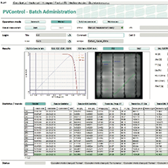
Its main applications in solar cell production are quality sorting and identification of processes that cause defects. For quality sorting, cells containing different defects exceeding a certain severity shall be sorted into lower quality bins. For the detection of deficient production steps, statistics on different defect categories are required. To obtain the relevant numbers, typically an EL evaluation pipeline is implemented (figure 1). In the first step, the image is recorded using optimised hardware settings including gain, image acquisition time and bias applied to the cell under evaluation. Step 2 comprises image pre-processing such as rectification, defect pixel removal or filtering. In step 3, segmentation of the pre-processed image and feature extraction provide a list of defect candidates and their features. Filtering of defect candidates based on their features provides the defects of interest in step 4. Finally, the last step comprises an evaluation of the EL information of the whole cell under test in order to assign a BIN class. Please note that the image analysis techniques employed for the different steps might differ between implementations.